28nm is the nominal resolution of the scanner. The chips that can be made with a single exposure. In that measure no ASML DUV scanner is 7nm either. The physics of 193nm light makes it impossible for any DUV scanner to have a nominal resolution of 7nm. 7nm chips are made using DUV by exposing 4 times at a 28nm resolution. The same quad patterning techniques allows 22nm chips to be made with a 90nm machine.
The name is also misleading 7nm chips aren't sub 9nm. TSMC's 7nm chips are physically 10nm. The marketing names haven't matched for years. It all started when TSMC sold 20nm FinFET under 16nm branding as they believed the addition of FinFET gave it 16nm performance. Then the entire industry adjusted their naming conventions to match with TSMC.
SMIC, Huawei didn't get to where they are by compromising. They never would've bought the Chinese domestic alternatives if not for sanctions. Price doesn't matter in this industry, what they're looking for is the best in the market. This is not the type of capital equipment that subsidies can sell. Which is why when US scanner manufacturers couldn't compete with ASML, they completely failed as economically viable businesses and their assets were sold off.
China prepared for this 17 years ago. They launched the "02 Special Project" all the way back in 2006. The companies established by those grants have existed years before the sanctions. They were able to develop the products but selling them was another thing entirely, until the sanctions hit causing a massive boom in their revenue. People forget that it was market conditions that killed GlobalFoundries 7nm effort not technical issues. The same reason UMC gave up on anything more advanced than 14nm. Sanctions created the inevitability of Chinese 7nm by wedding the world's largest telecom equipment vendor, Huawei to SMIC.
It's an amusing coincidence that by the time ASML will no longer be granted export licenses for their 5nm capable DUV scanners, the NXT:2000i and above, SMEE will be selling a 7nm capable scanner, the SSA/800-10W. A machine easily comparable to the NXT:1980Di that TSMC used to develop their N7 process. The fact that the NXT:1980Di and anything less advanced than it isn't going to be export restricted is an implicit acknowledgement of the Chinese capability of making competing machines.
5nm capable DUV scanners, such as the SSA/900 still in development, might be a requirement for SMIC N+2 however as the "7nm" Kirin 9000S is only 2% larger than the TSMC N5 made Kirin 9000. That suggest a density far exceeding anything any other foundry has been capable of with just DUV, such as Intel 7 or TSMC N7/N7P.
Applied Materials and LAM are less of an issue. AMEC has been selling 5nm etching systems to Samsung and TSMC for years.
TSMC made Kirin 9000 ran out in 2021, P50 Pro was the last phone to use it and the Kirin 820 ran out in 2022. It's only the 5G base stations that still use TSMC made HiSilicon chips.
Although I'd say these channels are more accurately described as apolitical analysis based on facts.
The only Nintendo console I ever had was a Famiclone so I don't really have much nostalgia for their games.
It's just Nintendo ROMs that are disappearing. It's still easier than ever to find even the most obscure classic PC games on abandonware sites and GOG compilation torrents. It's also only the SEO abusing ROM sites that are vulnerable to Nintendo's attacks. Complete ROMsets for their consoles can still be obtained through torrents, Vimm.net, and the r/ROMs megathread especially for the older cartridge consoles.
Emulating a current gen Nintendo console has never been as good as it is for Switch emulators. Any new PC can emulate Switch Triple As at full speed. Android is getting builds of the Yuzu emulator and mobile SOCs have enough power to run less demanding titles. When a lot people who don't even own a Switch can play Tears of the Kingdom, Nintendo is understandably trying to crack down. The portable aspect of the Switch is no longer a unique advantage. It used to be just GPD making those handheld PCs now every brand is trying to compete in that form factor.
Honestly I think the state of emulation in general is experiencing a golden age.
Retroid, Anbernic and AYN are making hardware that is a better solution for most people than trying to jailbreak and refurbish old original portable consoles. The screens, the analogs and the buttons they use are as good if not better than the first party hardware. Unlike bulky handheld PC, their Linux or Android based emulation handhelds are still in the same size and weight class as the PSP.
A couple years ago the Xbox 360 and PS3 emulators were basically just experimental demos. They weren't stable enough to actually finish any game on and most CPUs weren't fast enough to run them at full speed. They're still hit and miss but the list of playable titles will only ever grow.
It has come to the point that the PC can play everything. All previous gen consoles aside from the OG Xbox have emulators at a playable state. There are almost no current gen console exclusives anymore as the PC is getting ports of PS4/PS5 exclusives, the XBone/Series never had any to begin with, and of coarse the aforementioned Switch emulation.
That's based on TSMC's own test chip not an actual customer's. 17.92 mm² is incredibly tiny when SoCs, CPUs and GPUs range in size from 100 to 600 mm² increasing the proportion of chips with defects as the number of chips on the wafer drops.
From that very article
In that case, let us take the 100 mm2 die as an example of the first mobile processors coming out of TSMC’s process. Again, taking the die as square, a defect rate of 1.271 per cm2 would afford a yield of 32.0%.
As TSMC themselves designed the chip, they definitely followed all their design rules for that process to maximize yield. No customer would do that.
Anand explains this in one of his articles.
But have no fear. What normally happens is your foundry company will come to you with a list of design rules and hints. If you follow all of the guidelines, the foundry will guarantee that they can produce your chip and that it will work. In other words, do what we tell you to do, and your chip will yield.
The problem is that if you follow every last one of these design rules and hints your chip won’t be any faster than it was on the older manufacturing process. Your yield will be about the same but your cost will be higher since you’ll bloat your design taking into account these “hints”.
Generally between process nodes the size of the wafer doesn’t change. We were at 200mm wafers for a while and now modern fabs use 300mm wafers. The transistor size does shrink however, so in theory you could fit more die on a wafer with each process shrink.
The problem is with any new process, the cost per wafer goes up. It’s a new process, most likely more complex, and thus the wafer cost is higher. If the wafer costs are 50% higher, then you need to fit at least 50% more die on each wafer in order to break even with your costs on the old process. In reality you actually need to fit more than 50% die per wafer on the new process because yields usually suck at the start. But if you follow the foundry’s guidelines to guarantee yield, you won’t even be close to breaking even.
The end result is you get zero benefit from moving to the new process. That’s not an option for anyone looking to actually use Moore’s Law to their advantage. Definitely not for a GPU company.
The solution is to have some very smart people in your company that can take these design rules and hints the foundry provides, and figure out which ones can be ignored, and ways to work around the others. This is an area where ATI and NVIDIA differ greatly.
TSMC N7, N7P and Intel 7 don't use EUV. It's all quad patterned DUV. DUV lithography has been in use since the 1990s going from 800nm to N7P.
Every single node after TSMC's so called 16nm has been all marketing. It would've more accurate to call TSMC 16FF as 20nm FinFET. This is why Intel brands what they themselves called 10nm as Intel 7 to bring their marketing more in line with TSMC's.
SMIC N+1 has a density of 89 million of transistors per mm² while TSMC N7 has 91.2. TSMC 10FF and Samsung 10LPP only offer slightly more than half that density.
She lit the first match, and saw her lost motherland;
She lit the second match, and saw its great ideals;
She lit the third match, and saw her motherland's aerospace pioneers driven by those ideals;
She lit the fourth match, and saw her long dead little sister Buran.
She was afraid that as the matches went out, these dreams would be lost forever; so she lit all she had left wishing that they stayed with her.
In the end, she died with a smile.
No one knows what beautiful scene she saw at the last moment of her life.【22.3.3-4】
The Russians see East Ukrainians as Russians.
The US media othered Iraqis and Afghans so much that a certain group of Americans started attacking other Americans that were Muslims and/or of west/south-Asian descent.
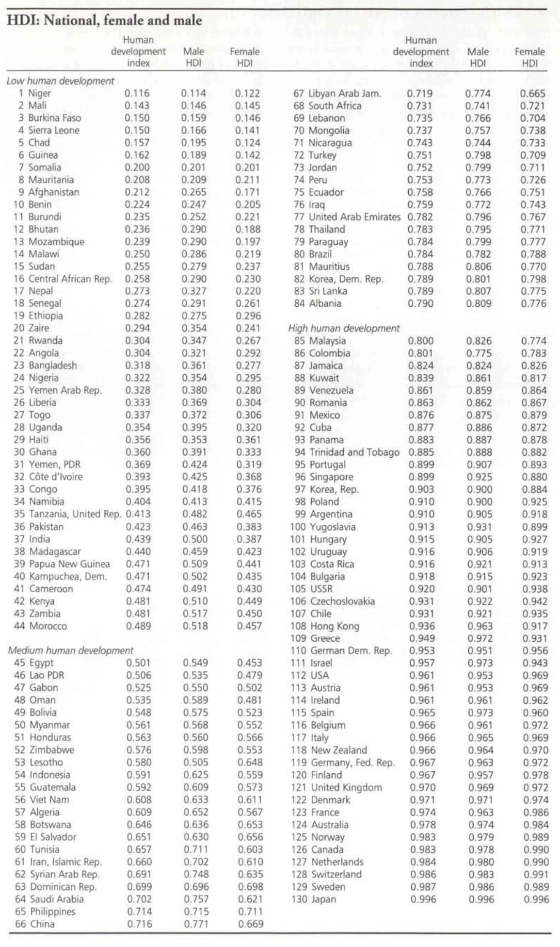
The 1990 HDI of DPRK was higher than the Philippines, which is arguably more representative of what a US colony would actually look like when the Americans do not fund a significant portion of the state budget as they did in Park era SK.